../ --> Go back to Homepage
Conductivity Based Atomic Force Microscope v0.0.1
By: Vincent Banek --- Date: 3/8/25
(Original Report for college course: May 2024)
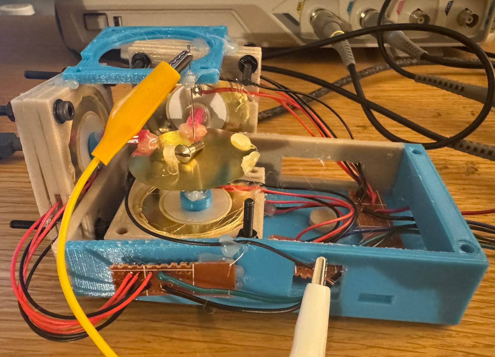
Notes: I originally made this project for my subsystems college course (CET4711) in spring 2024, This is my 2nd attempt of making an AFM, I also tried making one in high school but there was some misunderstandings about the arduino MCU, that caused it not to work well, this article is based on my project report for my college course, because of time constraints, I could not finish the upper half of the AFM, the upper half is for the probe that scans the item placed under it, to demonstrate its function, I hot glued a needle to a scrap plastic part to place the needle pointing down, I then needed to find a metal sample that would both fit the gap and produce a interesting image, even though I planned on some kind of film or semiconductor, I used a screw since its not that springy and the gap was to large for the type of item I actually wanted to scan.
Now that I graduated I plan on restarting the project, to function better and expand on it, for use on semiconductors, I also think that living cells could be interesting, after fixing the frame, my first modification planned is a optical microscope in order to see a image of the sample optically and via C-AFM, side by side, and see if the oscillation is correct.
I plan on releasing the code and CAD files on github but want to refactor the CAD files and rewrite the code for the Arduino Minima first to address some problems caused by the limited memory on the UNO.
1 Objectives
- Research Project
- Make a Conductivity based AFM (Atomic Force Microscope)
- Construct the rig that scans the object
- Create Code for it, and Wire it.
- Generate Image of the area scaned
- prove components work together and are useful.
2 Component List
- Arduino Mega.
- 2 10kΩ Resistor
-
1 47uF Capicitor, One 1000uF one(1000uF is all I had, but it worked enough, under 47uF is to small)
-
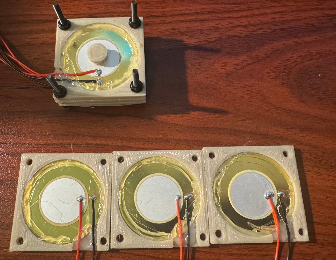
10 47mm Piezo Disc (Marketed for Hybrid Acoustic Guitar Pickups)Used to make 3 actuatorsOne is actually used as a conductive platform and isn’t active.
- wires and breadboard, solder and phototype board to expand and anchor wires.
- a needle to be used as probe
- Hot glue and hot glue gun
- 10 30mm M3 Screws, with 10 M3 nuts, and 20 M3 Washers
- A spring to put platform on so it can move freely, I used 7X12 5mm compressing spring.
- 3D printer for 3D printing parts
- 5V from USB.
- Computer with Arduino IDE, and to run the image program on Processing
- A condutive item to scan, I choose the thread of a small screw.
3 Choosing Project/Research
4 Procedure
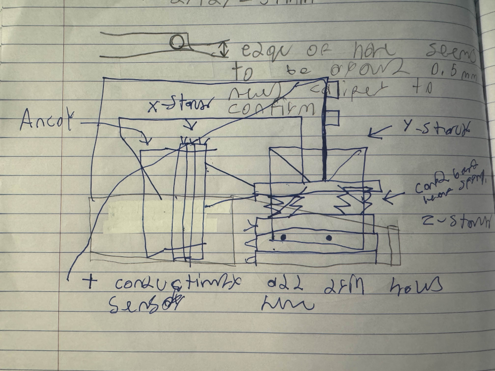
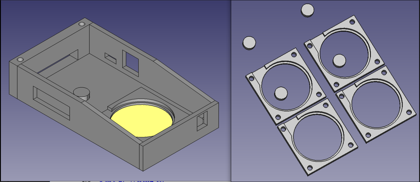
4.1 Part 1: Designing and building the rig:
4.2 Part 2: Writing Code for it:
void ProbeCord(char movx, char movy) {
  // had to make the code downscale by a quarter for it to fit on arduino.
  int qmovx = movx*4;
  int qmovy = movy*4;

  moveprobe(qmovx, qmovy, 255);
  char qnn = constrain(map(analogRead(probe), lower, upper, 0, 255), 0, 255);
  moveprobe(qmovx+1, qmovy, 255);
  char qpn = constrain(map(analogRead(probe), lower, upper, 0, 255), 0, 255);
  moveprobe(qmovx, qmovy+1, 255);
  char qnp = constrain(map(analogRead(probe), lower, upper, 0, 255), 0, 255);
  moveprobe(qmovx+1, qmovy+1, 255);
  char qpp = constrain(map(analogRead(probe), lower, upper, 0, 255), 0, 255);
  ImageBuffer0[movx][movy] = (qnn+qpn+qnp+qpp)/4;
  digitalWrite(Zenable, LOW);
  digitalWrite(XYenable, LOW);
}
void TakeImage() {
  for(int yscan=0; yscan < 64; yscan++) {
    for(int xscan=0; xscan < 64; xscan++) {
      ProbeCord(xscan, yscan);
    }
    analogWrite(piezoX, 0);
    delay(RCDelay); // Give time for voltage to go down.
  }
}
4.3 Part 2: Wiring it:
4.4 Part 3: Place object and Calibrate Machine
4.5 Part 4: Getting Image:
5 Diagrams
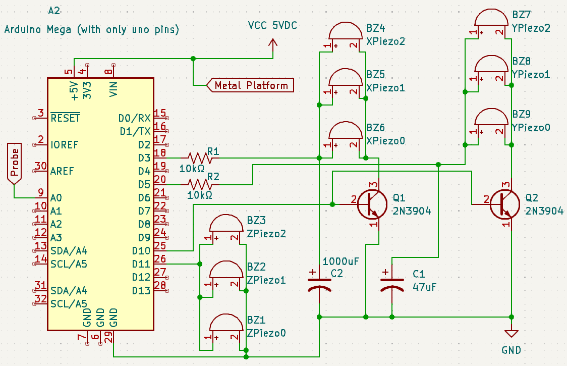
5.1 Hardware: (Schematic Diagram)
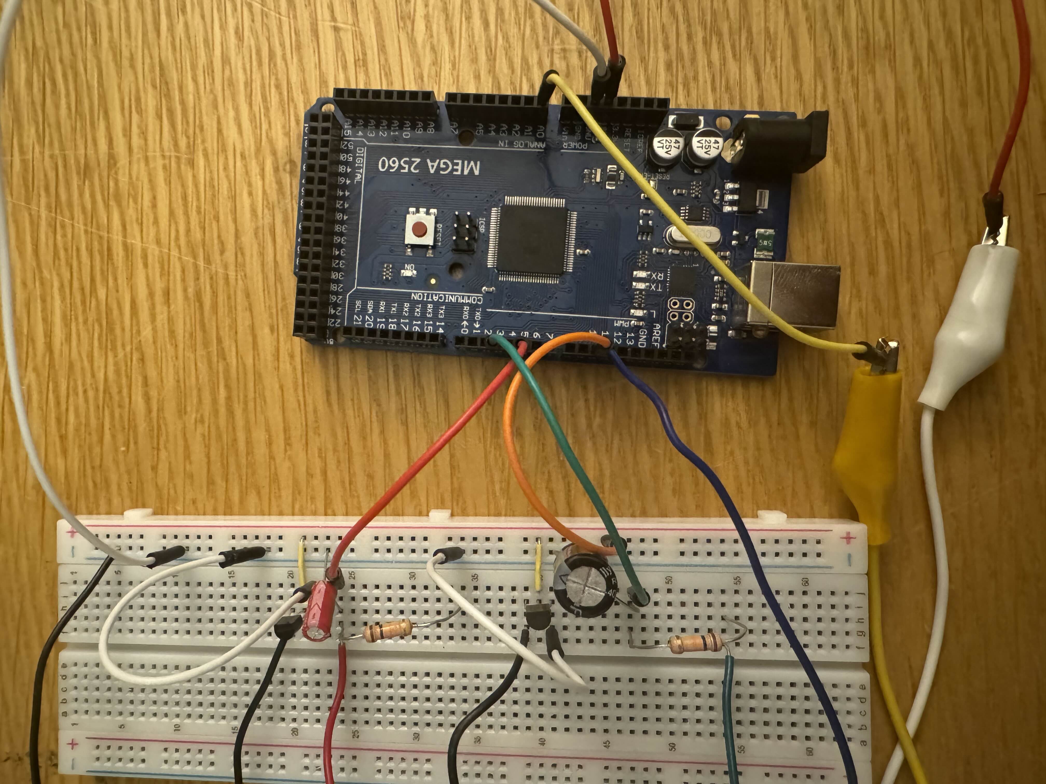
5.2 Hardware: (Picture of Electrical Circuit)
Sub-Systems Used:
- Microcontroller: Arduino Mega with ATMega2560-16AU (16Mhz, TQFP Package)
- Low Level: Serial Communcation
- High Level: USB Communication
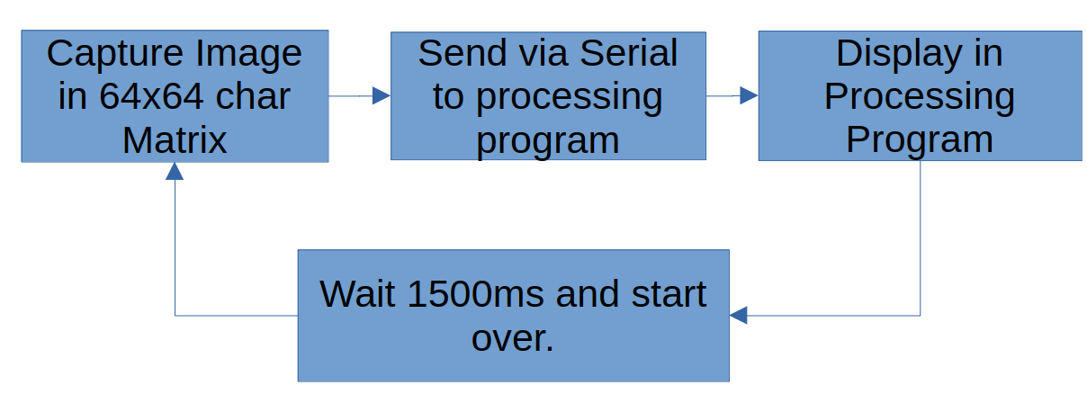
- Software: Block Diagram
- Explains the loop of the system in a block diagram.
6 Source Code
char ImageBuffer0[64][64];
#define piezoX 3 // For X axis
#define piezoY 5 // For Y axis
#define piezoZ 7 // Not used if 255 only
// May be expanded for depth later
#define XYenable  10
#define Zenable   11 // Connect Piezo Z directly here
// it stays at 255 or 5V so this allows me make
// the circuit simpler
#define probe     A0
// Rewrite this during your calibration process. leave * 4, I prefer to use
// 0 to 255 but did not went to change code for 255, so left it like this.
int upper = 175 * 4; // Sets higher expected value, default is 255.
int lower = 100 * 4; // Sets lower expected value, default is 0.
// sets delay in ms to allow RC filter to charge.
int RCDelay = 10;
void setup() {
  // init serial
  Serial.begin(115200);
  // initialize digital pin LED_BUILTIN as an output.
  pinMode(LED_BUILTIN, OUTPUT);
  pinMode(piezoX, OUTPUT);
  pinMode(piezoY, OUTPUT);
  pinMode(piezoZ, OUTPUT);
  pinMode(XYenable, OUTPUT);
  pinMode(Zenable, OUTPUT);
  pinMode(probe, INPUT);
}
int GetValue(int getx, int gety){
    return ImageBuffer0[getx][gety];
}
void SendViaSerial() {
  Serial.print("."); // Signals new image.
  for(int ysend=0; ysend < 64; ysend++) {
    Serial.print(GetValue(0, ysend));
    for(int xsend=1; xsend < 63; xsend++) {
      Serial.print(GetValue(xsend, ysend));
      Serial.print(","); // next value
    }
    // next row
    Serial.println(GetValue(64, ysend));
  }
  Serial.print(";"); // to tell the system its done.
}
void moveprobe(char movx, char movy, char movz) {
  digitalWrite(Zenable, LOW);
  digitalWrite(XYenable, LOW); // Wait until cords are set.
  analogWrite(piezoX, movx); // go to cords
  analogWrite(piezoY, movy);
  analogWrite(piezoZ, movz);
  delay(1); // allow rc filter to get to right voltage.
  digitalWrite(XYenable, HIGH);
  delay(1); // very short delay, so probe does not scratch.
  digitalWrite(Zenable, HIGH);
}
void ProbeCord(char movx, char movy) {
  // had to make the code downscale by a quarter for it to fit on arduino.
  int qmovx = movx*4;
  int qmovy = movy*4;

  moveprobe(qmovx, qmovy, 255);
  char qnn = constrain(map(analogRead(probe), lower, upper, 0, 255), 0, 255);
  moveprobe(qmovx+1, qmovy, 255);
  char qpn = constrain(map(analogRead(probe), lower, upper, 0, 255), 0, 255);
  moveprobe(qmovx, qmovy+1, 255);
  char qnp = constrain(map(analogRead(probe), lower, upper, 0, 255), 0, 255);
  moveprobe(qmovx+1, qmovy+1, 255);
  char qpp = constrain(map(analogRead(probe), lower, upper, 0, 255), 0, 255);
  ImageBuffer0[movx][movy] = (qnn+qpn+qnp+qpp)/4;
  digitalWrite(Zenable, LOW);
  digitalWrite(XYenable, LOW);
}
void TakeImage() {
  for(int yscan=0; yscan < 64; yscan++) {
    for(int xscan=0; xscan < 64; xscan++) {
      ProbeCord(xscan, yscan);
    }
    analogWrite(piezoX, 0);
    delay(RCDelay); // Give time for voltage to go down.
  }
}
// the loop function runs over and over again forever
void loop() {
  digitalWrite(LED_BUILTIN, HIGH);  // show that program starts.

  TakeImage(); // Take the Atomic Force Image
  // send over serial

  SendViaSerial();
  digitalWrite(LED_BUILTIN, LOW); // To show speed of program
  delay(1500); // wait a while before next image.
}
import processing.serial.*;
Serial myPort;  // Create object from Serial class
int val;      // Data received from the serial port
String SerialMsg;
void setup()
{
  // 64 by 64 resolution scaled up by 10.
  size(640, 640);
  // Assumes 1st Serial Port
  String portName = Serial.list()[0];
  myPort = new Serial(this, portName, 115200);
  myPort.bufferUntil(’;’);
}
void draw()
{
  String[] rows = new String[65];
  String[] columns = new String[65];
  if (SerialMsg != null) {
   rows = split(SerialMsg, ’\n’);
    for(int i=0; i<rows.length; i++) {
     columns = split(rows[i], ’,’);
     for(int j=0; j < columns.length; j++) {
       fill(int(columns[j]));
       rect(j*10, i*10, 10, 10);
      }
    }
    SerialMsg = null;
  }
}
void serialEvent(Serial myPort) {
  SerialMsg = myPort.readStringUntil(’;’);
}
7 Measurements
-
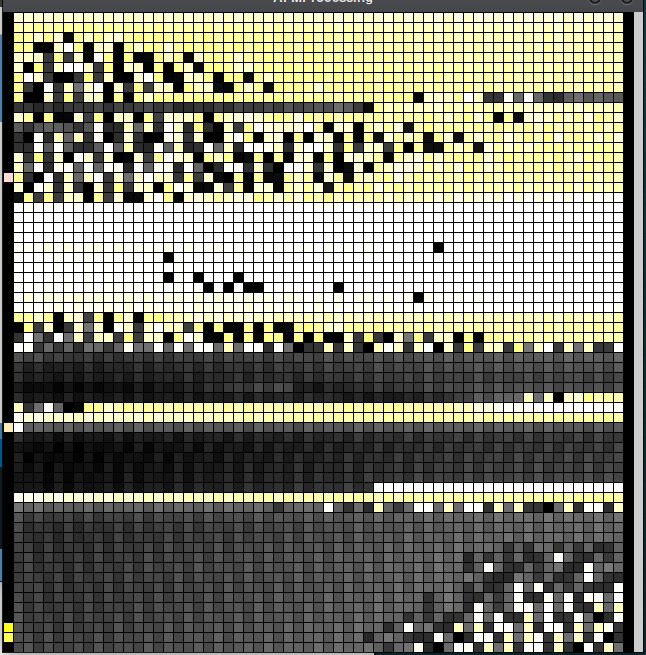
Processing Image Generation
This is likely shows the thread of the screw with some dust.
-
Serial Monitor
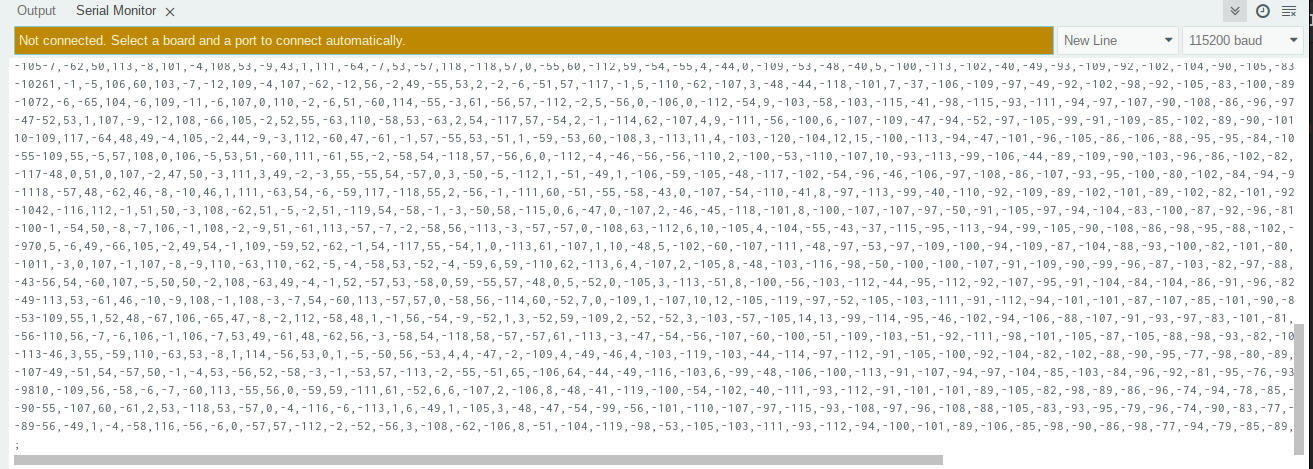 This is the format used for the serial communcation.
8 Troubleshooting
9 Discussion
9.1 Data Input Sub-Systems:
- Hardware:
-
Sensor(s) used for data input:Just a probe connected to A0 and a platform connected to 5V.
-
Interface Circuit(s):None
-
void ProbeCord(char movx, char movy) {
  // had to make the code downscale by a quarter for it to fit on arduino.
  int qmovx = movx*4;
  int qmovy = movy*4;
  moveprobe(qmovx, qmovy, 255);
  char qnn = constrain(map(analogRead(probe), lower, upper, 0, 255), 0, 255);
  moveprobe(qmovx+1, qmovy, 255);
  char qpn = constrain(map(analogRead(probe), lower, upper, 0, 255), 0, 255);
  moveprobe(qmovx, qmovy+1, 255);
  char qnp = constrain(map(analogRead(probe), lower, upper, 0, 255), 0, 255);
  moveprobe(qmovx+1, qmovy+1, 255);
  char qpp = constrain(map(analogRead(probe), lower, upper, 0, 255), 0, 255);
  ImageBuffer0[movx][movy] = (qnn+qpn+qnp+qpp)/4;
  digitalWrite(Zenable, LOW);
  digitalWrite(XYenable, LOW);
}
The above code averages the values from A0 in a 4x4 area and stores it, in the 64x64 char matrix.
9.2 Data Processing/Data Storage Subsystems:
- Hardware:
-
Micro-controller:Arduino Mega: with Atmega2560 chip,
- Runs at 16Mhz
- Separate USB to Serial Chip (On board)
- 54 Digital Pins
- 15 PWM Pins
- 16 Analog input pins.
- Software:
- Data Processing operation(s):
-
int qmovx = movx*4; int qmovy = movy*4; moveprobe(qmovx, qmovy, 255); char qnn = constrain(map(analogRead(probe), lower, upper, 0, 255), 0, 255); moveprobe(qmovx+1, qmovy, 255); char qpn = constrain(map(analogRead(probe), lower, upper, 0, 255), 0, 255); moveprobe(qmovx, qmovy+1, 255); char qnp = constrain(map(analogRead(probe), lower, upper, 0, 255), 0, 255); moveprobe(qmovx+1, qmovy+1, 255); char qpp = constrain(map(analogRead(probe), lower, upper, 0, 255), 0, 255); ImageBuffer0[movx][movy] = (qnn+qpn+qnp+qpp)/4; - theres both 4 maping functions, addition, multiplication, and division here, to get the 4 values and sum them up.
- Data Storage operation(s):
- Size of FLASH memory (used / total) for storing program code (Bytes): 4734 Bytes
-
Size of RAM (used / total) for storing variables (Bytes):4290 Bytes
9.3 Data Output Sub-systems:
- Hardware:
- Output device(s) used: 3 piezo actuators made up of 3 stacked piezo disk for X, Y & Z.
- Interface Circuit(s): 2 RC circuits made with 47uF, 1000uF Capitors and 2 10kΩ Resistors, for XY connected to 3 & 5, with ground osculated via NPN transistor to allow RC circuits to charge at right voltage connected to pin 10, Z is connected directly between pin 11 and ground.
-
Software:
void moveprobe(char movx, char movy, char movz) {
  digitalWrite(Zenable, LOW);
  digitalWrite(XYenable, LOW); // Wait until cords are set.
  analogWrite(piezoX, movx); // go to cords
  analogWrite(piezoY, movy);
  analogWrite(piezoZ, movz);
  delay(1); // allow rc filter to get to right voltage.
  digitalWrite(XYenable, HIGH);
  delay(1); // very short delay, so probe does not scratch.
  digitalWrite(Zenable, HIGH);
}
It sets the position by giving the RC circuits a PWM signal which is defined 0 to 255, then turning the ground on to allow it to power the piezo actuators.Zenable lifts the platform, I decided to bypass PiezoZ to make the circuit simple since it stays at 255.
9.4 Data Communications Subsystems:
9.5 Hardware:
-
Output Communcation Interface circuit(s) used:Just a USB-B cable using Arduinos built in USB controller, It use’s a FTDI chip to convert USB signals to TTL UART Serial.
-
Software:arduino
void SendViaSerial() {
  Serial.print("."); // Signals new image.
  for(int ysend=0; ysend < 64; ysend++) {
    Serial.print(GetValue(0, ysend));
    for(int xsend=1; xsend < 63; xsend++) {
      Serial.print(GetValue(xsend, ysend));
      Serial.print(","); // next value
    }
    // next row
    Serial.println(GetValue(64, ysend));
  }
  Serial.print(";"); // to tell the system its done.
}
This code sends the data to processing so it can be inteprated as a image, it works by running a for loop similar to scanning the object, begining with a ’.’ to start, signeling a new row with a new line, and ending it with ’;’. GetValue just concerts the output to int or the arduino would send it as a character instead of a 8 bit number defined in ASCII. this is because char is really short for characters but can also be used for 8bit numbers because in memory its the same thing.